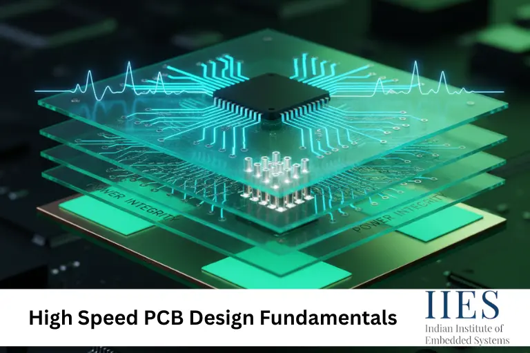
What Makes a PCB “High Speed”?
A
PCB is considered high speed when the signal rise time is comparable to the propagation delay of the trace. When this condition is met, the PCB behaves as a transmission line rather than a simple interconnection.
At this point, High Speed PCB Design techniques such as impedance control, termination, stack-up planning, and disciplined routing become essential to prevent signal degradation, timing errors, and EMI issues.
Common Interfaces That Require High Speed PCB Design
Many modern digital and RF interfaces rely heavily on proper
High Speed PCB Design, including:
- USB 2.0, USB 3.0, USB 3.1, and USB Type-C
- HDMI and DisplayPort
- Ethernet (100 Mbps, 1 Gbps, 10 Gbps, and higher)
- PCI Express (PCIe) for CPUs, GPUs, and peripherals
- SATA and eSATA storage interfaces
- DDR, DDR2, DDR3, DDR4, and DDR5 memory buses
- LVDS (Low-Voltage Differential Signaling)
- MIPI camera and display interfaces
- High-speed SPI and QSPI
- Wi-Fi, Bluetooth, and other GHz-range RF signal paths
Each of these interfaces requires strict routing rules, impedance control, and careful High Speed PCB Design planning.
Key Layout Concepts in High Speed PCB Design
A reliable High Speed PCB Design layout depends on several core principles:
- Controlled trace width and spacing
- Consistent and continuous reference planes
- Proper routing topology
- Minimal impedance discontinuities
Following proven High Speed PCB Design layout rules helps reduce distortion, timing errors, and EMI, forming the foundation of successful high-speed board designs.
Choosing the Right Materials for High Speed PCB Design
Standard FR-4 material may be insufficient for advanced High Speed PCB Design, especially at multi-GHz frequencies. Dielectric loss and Dk variation can cause signal attenuation and phase distortion.
Selecting low-loss, stable PCB materials is critical in professional High Speed PCB Design, particularly for interfaces such as PCIe, USB 3.x, HDMI, and DDR memory.
Key Design Considerations in High Speed PCB Design
The performance of High Speed PCB Design depends on careful control of signal behavior, power delivery, and electromagnetic compatibility.
- Controlled Impedance
Controlled impedance ensures traces match the required characteristic impedance, minimizing reflections and maintaining signal integrity in High Speed PCB Design.
- Signal Integrity
Signal integrity is the core objective of High Speed PCB Design. Noise, reflections, and attenuation can cause data errors and system instability.
- Crosstalk Reduction
Crosstalk occurs when signals couple into adjacent traces. Increasing spacing, routing orthogonally on adjacent layers, and using ground shielding are key High Speed PCB Design techniques.
- Layer Stack-Up Design
A well-planned stack-up improves impedance control, reduces noise coupling, and provides clean return paths for High Speed PCB Design.
- Power Integrity
Stable power delivery is essential in High Speed PCB Design. Proper decoupling, solid power planes, and low-impedance grounding prevent voltage noise and random failures.
- Return Path Control
High-speed signals follow the path of least impedance. Maintaining continuous return paths is a fundamental High Speed PCB Design requirement to reduce EMI.
- Differential Pair Routing
Differential signals require matched impedance, spacing, and length. This is widely used in High Speed PCB Design for USB, HDMI, Ethernet, and PCIe.
- Via and Stub Management
Vias introduce impedance discontinuities. Minimizing vias, reducing stubs, and using back-drilling improve High Speed PCB Design signal quality.
- Timing and Length Matching
Careful length matching prevents skew in High Speed PCB Design, especially for memory and high-speed serial buses.
- EMI and EMC Control
Proper grounding, shielding, and layout discipline are essential in High Speed PCB Design to meet regulatory compliance.
- Termination Techniques
Series, parallel, and differential termination prevent reflections by matching impedance in High Speed PCB Design.

USB PCB Design Guidelines and Other High-Speed Interfaces
Interfaces such as USB, HDMI, PCIe, and DDR demand strict High Speed PCB Design rules, including differential impedance matching, minimal skew, and controlled trace geometry. Following USB PCB design guidelines ensures compliance and long-term reliability.
Practical Challenges in High Speed PCB Design
In real-world projects, most failures occur due to layout and manufacturing oversights in High Speed PCB Design, not schematic errors.
Common challenges include:
- Signal integrity issues discovered after fabrication
- Impedance mismatches from stack-up changes
- Excessive vias in dense routing
- Broken return paths near connectors
- Length matching difficulties
- Crosstalk in high-density areas
- Power integrity ignored during layout
- EMI failures during compliance testing
- FR-4 limitations at high frequencies
- Poor communication with PCB manufacturers
Addressing these challenges early greatly improves High Speed PCB Design success.
Conclusion
High Speed PCB Design requires a strong understanding of signal behavior, material properties, layout discipline, and EMI control. By applying proven High Speed PCB Design rules, selecting appropriate materials, following USB PCB design guidelines, and maintaining strong signal integrity practices, engineers can design robust, manufacturable, and high-performance electronic products.


