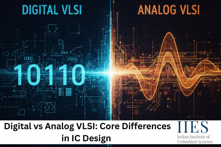
Digital VLSI vs Analog VLSI – Quick Overview
| Aspect | Digital VLSI | Analog VLSI |
|---|
| Signal Type | Discrete (0, 1) | Continuous |
| Transistor Usage | Switching | Amplification |
| Noise Tolerance | High | Low |
| Design Automation | Very high | Limited |
| Scaling Benefits | Strong | Limited |
| Design Difficulty | Moderate | High |
| Best For | Computing & control | Real-world signal interface |
What is Digital VLSI?
Digital VLSI deals with circuits that operate on binary logic, where information is represented using two voltage levels: logic 0 and logic 1.
These circuits form the backbone of modern computing systems.
Key Features of Digital VLSI
- Uses discrete voltage levels
- High tolerance to noise and process variations
- Scales efficiently with advanced CMOS nodes
- Strong support from automated EDA tools
Common Applications
- Microprocessors and microcontrollers
- SRAM, DRAM, Flash memory
- GPUs and AI accelerators
- Digital control logic

What is Analog VLSI?
Analog VLSI focuses on circuits that process continuous signals, where voltage or current can take any value within a range.
These circuits directly interface with the physical world.
Key Features of Analog VLSI
- Continuous voltage or current levels
- Strong dependence on transistor characteristics
- Requires precise biasing and careful layout
- Highly sensitive to noise, mismatch, and temperature
Common Applications
- Audio and RF circuits
- Power management ICs (PMICs)
- Sensor and biomedical interfaces
- ADC and DAC blocks
1. Nature of Signals
Digital VLSI
Digital circuits operate on two logic levels:
Typical voltage ranges:
- 0–0.8 V → Logic 0
- 2–5 V → Logic 1
Result:
Small variations in device parameters are masked, making digital circuits robust and reliable.
Analog VLSI
Analog circuits work with continuously varying signals in both time and amplitude.
Result:
Small changes in transistor parameters, noise, or temperature can significantly impact performance.
2. Transistor Operation and Biasing
Digital VLSI
- Transistors act as switches
- Operate mainly in cutoff and saturation
- Focus on speed, power, and area
Primary Goal:
Maximize switching speed and minimize energy per operation.
Analog VLSI
- Transistors act as amplifiers
- Typically biased in saturation region
- Matching and bias accuracy are critical
Primary Goal:
High gain, good linearity, and low noise.
3. Design Methodology
Digital IC Design Flow
- System specification
- RTL design (Verilog / VHDL)
- Logic synthesis
- Place and route
- Timing and power verification
Design Style:
Top-down and highly automated.
Analog IC Design Flow
- System-level modeling
- Transistor sizing
- Biasing and simulation
- Careful layout with matching constraints
- Post-layout verification
Design Style:
Bottom-up and largely manual.
4. Noise Sensitivity
Digital VLSI
- Can tolerate thermal noise, crosstalk, and supply noise
- Correct operation ensured as long as noise margins are met
Analog VLSI
Highly sensitive to:
- Thermal noise
- Flicker (1/f) noise
- Power supply variations
Noise reduction is one of the biggest challenges in analog design.
5. Performance Metrics
Digital VLSI Metrics
Analog VLSI Metrics
- Gain
- Bandwidth
- Linearity
- Noise figure and SNR
6. Technology Scaling Impact
Digital VLSI
- Major beneficiary of scaling
- Higher speed and density
- Lower cost per function
Digital circuits continue to improve with smaller nodes.
Analog VLSI
- Reduced voltage headroom
- Lower intrinsic gain
- Increased design complexity
Analog performance does not scale as efficiently as digital.
7. Verification and Testing
Digital VLSI
- Automated simulation and verification
- Structured testing methodologies
- Easier fault detection
Analog VLSI
- Extensive corner and Monte Carlo simulations
- Manual and instrument-based testing
- Fault detection is more complex
8. Real-World Industry Example (E-E-A-T Boost)
In a smartphone SoC:
- Analog blocks: RF transceiver, PMIC, audio codec
- Digital blocks: CPU, GPU, DSP, AI accelerator
This combination forms a mixed-signal chip, which dominates modern semiconductor products.
9. Mixed-Signal VLSI
Most modern ICs are mixed-signal, combining both domains:
- Analog front-end for sensing and signal conditioning
- Digital back-end for computation and control
Common in:
Top 5 VLSI Interview Questions Asked by Leading VLSI Companies
1. Which is harder: Digital or Analog VLSI?
Answer:
Analog VLSI is harder due to its strong dependence on transistor physics, noise, matching, and layout, while digital VLSI benefits from abstraction and automation.
2.Why does digital VLSI scale better than analog VLSI?
Answer:
Digital circuits gain speed and density with scaling, whereas analog circuits suffer from reduced voltage headroom and lower intrinsic gain.
3.Why is layout more critical in analog VLSI than in digital VLSI?
Answer:
Analog performance is highly sensitive to device matching and parasitics, while digital circuits are more tolerant to layout variations.
4.How do noise requirements differ in digital and analog VLSI?
Answer:
Digital circuits only require noise to stay within noise margins, whereas analog circuits must minimize noise to preserve signal integrity.
5. What is mixed-signal VLSI?
Answer:
Mixed-signal VLSI combines analog circuits for real-world signal interfacing with digital circuits for computation and control.
Final Thoughts
Digital and analog VLSI serve different but equally important roles in IC design.
Digital VLSI enables large-scale computing and automation, while analog VLSI connects silicon to the real world.
Engineers skilled in both domains, especially mixed-signal design, are among the most valued professionals in the semiconductor industry.