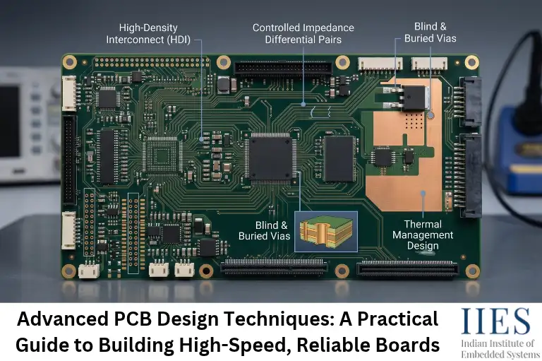
What Is Advanced PCB Design (and When Do You Need It)?
In short: Advanced PCB design treats the board as an electrical, thermal, and manufacturing system, not just a wiring diagram. You decide the stack-up, return paths, power network, and assembly process on purpose instead of hoping they work out.
You need advanced techniques when:
- Signal edges are fast (rise times below roughly 2 to 3 ns), even if the clock is slow
- The board uses USB, Ethernet, SDRAM/DDR, HDMI, MIPI, or PCIe
- BGA or fine-pitch QFN parts force dense routing
- A switching regulator, motor driver, or relay shares the board with sensitive analog or RF circuits
- The product must pass EMC testing, run hot, or survive a harsh environment

Basic vs advanced PCB design at a glance
Area | Basic approach | Advanced approach |
Layers | 1 to 2 layers | 4 to 12+ layers with a planned stack-up |
Routing | Connect nets and pass DRC | Impedance-controlled, length-matched, return-path aware |
Power | Wide traces | Planes, target impedance, tuned decoupling |
Vias | Through-hole only | Blind, buried, microvias, via-in-pad where justified |
Checks | ERC and DRC | DRC plus SI/PI checks, thermal review, DFM/DFA/DFT review |
The one idea behind most of this guide
- Signal quality depends on edge rate (rise time), not clock frequency
- Rule of thumb: bandwidth ≈ 0.35 ÷ rise time. A 1 ns edge carries useful energy up to about 350 MHz (some engineers use 0.5 ÷ rise time, which gives 500 MHz)
- On FR-4, signals travel about 6 to 7 ps per mm
- A common rule says a trace behaves like a transmission line once its delay exceeds about one-sixth of the rise time
Worked example: For a 1 ns edge, 1000 ps ÷ 6 ≈ 167 ps. At about 6.5 ps/mm, that’s roughly 25 mm (about 1 inch). Any trace longer than that needs impedance control, proper termination, and a clean return path.
That’s why a 16 MHz MCU can still cause EMI. The clock is slow, but its GPIO edges may not be.
Technique 1: Plan the Layer Stack-Up Before You Place a Single Part
In short: Your stack-up decides impedance, crosstalk, EMI, and power-network quality. Fix it first, because it’s painful to change later.
Stack-up rules that work:
- Put every signal layer next to a solid reference plane (usually ground)
- Keep power and ground planes close together (thin dielectric) for free high-frequency capacitance
- Keep the stack-up symmetric around the centre so the board doesn’t warp during reflow
- Route adjacent signal layers in perpendicular directions
- Get the stack-up and dielectric data from your fab before calculating any trace width
- Choose high-Tg FR-4 (around 170 °C) for lead-free assembly, and move to low-loss laminates only when multi-GHz loss demands it
Example stack-ups
Layers | Typical order (top to bottom) | Best for |
4 | Signal / GND / Power / Signal | MCU boards, USB, basic IoT nodes |
6 | Signal / GND / Signal / Power / GND / Signal | Ethernet, mixed-signal, BGA MCUs and SoCs |
8 | Signal / GND / Signal / Power / GND / Signal / GND / Signal | DDR3/DDR4, dense SoCs, multiple high-speed buses |
Pro tip: If your board has several high-speed buses, a 4-layer stack is usually where the layout starts fighting back. Moving to 6 layers is often cheaper than the debugging time.
Technique 2: Use Controlled Impedance Routing
In short: Controlled impedance means choosing trace width, spacing, and dielectric height so a trace has a defined characteristic impedance (for example, 50 Ω). This prevents reflections that show up as ringing, overshoot, and data errors.
Think of a water pipe. If the pipe suddenly changes diameter, some of the flow sloshes backwards. A signal hitting an impedance change does the same thing.
Typical target impedances
Signal type | Typical target |
General high-speed single-ended, RF feed lines | 50 Ω |
USB 2.0 and USB 3.x pairs | 90 Ω differential |
Ethernet, LVDS, HDMI | 100 Ω differential |
Always cross-check with the chip’s datasheet or layout guide, since some interfaces (like DDR) specify their own values.
Microstrip, stripline, and coplanar waveguide
- Microstrip: outer-layer trace over a reference plane. Easy to probe and tune, but radiates more
- Stripline: inner-layer trace between two planes. Better shielded, slightly slower signal travel
- Coplanar waveguide with ground (CPWG): common for RF lines, with ground copper on both sides stitched by vias
Worked example: estimating trace width
A handy approximation for microstrip (from IPC-2141) is:
Z₀ ≈ [87 ÷ √(εr + 1.41)] × ln[5.98h ÷ (0.8w + t)]
Here h is dielectric height, w is trace width, t is copper thickness, and εr is the dielectric constant.
- Take εr = 4.2, h = 0.2 mm, w = 0.35 mm, t = 0.035 mm (1 oz copper)
- 87 ÷ √5.61 ≈ 36.7
- ln(1.196 ÷ 0.315) ≈ 1.33
- Z₀ ≈ 36.7 × 1.33 ≈ 49 Ω
Treat this as a sanity check. Use a field solver or your fab’s calculator for the final numbers.
How to apply it in your project
- Get the fab’s stack-up (dielectric thickness, Dk, copper weight)
- Calculate width and spacing with a field solver (most EDA tools include one)
- Create net classes and impedance rules in your EDA tool
- Add an impedance table and stack-up drawing to your fabrication notes
- Ask for impedance test coupons. A tolerance of ±10% is common
Technique 3: Route Differential Pairs and Match Lengths Properly
In short: Route pairs as a pair, match lengths where timing matters, and keep the path from driver to receiver as uninterrupted as possible.
Differential pair rules
- Keep spacing constant along the pair, and keep both traces the same length (minimal intra-pair skew)
- Bend both traces symmetrically
- Don’t route pairs across plane splits, slots, or gaps
- If a pair must change layers, use symmetrical vias and add a ground stitching via next to each signal via
- Place AC coupling capacitors side by side, close to the transmitter or connector, as the interface guide specifies
- Keep pairs away from noisy neighbours such as switching nodes, crystals, and clocks
Length matching for parallel buses
- Match lengths within a group (for example, data lines with their clock in SDRAM, SDIO, or a parallel LCD bus), not across the whole board
- Tune with serpentines: spacing of 3 to 4 times the trace width, gentle amplitude, no tight accordions
- Add the delay near the source of the mismatch
- Signals travel faster on outer layers than inner layers, so equal length is not always equal delay. Use delay-based tuning if your tool supports it
- Use the tolerances from the chip vendor’s layout guide, not generic numbers
Routing habits that pay off
- Prefer 45° bends or arcs. At low speed, 90° corners are mostly an etching concern, but they’re easy to avoid
- Minimise vias on fast nets. Each via adds inductance, capacitance, and possibly a stub
- For multi-gigabit links, consider blind vias or back-drilling to remove stubs
- Use series termination for point-to-point outputs. Pick a resistor so that resistor + driver output impedance ≈ trace impedance, and place it right next to the driver
Technique 4: Protect Return Paths and Control Crosstalk
In short: Every signal needs a return path, and at high frequency the return current flows directly underneath the trace. Break that path and you get EMI, crosstalk, and ringing.
Think of the signal as a car and the return current as the road back home. At low speed, the car can take any route. At high speed, only the shortest road, right under the trace, will do.
What breaks the return path
- Traces crossing a split or slot in the reference plane
- Layer changes without a nearby ground via
- Large via fields that turn a plane into Swiss cheese
- A reference that switches from GND to a power plane mid-route
How to control crosstalk
- Start with the 3W rule: centre-to-centre spacing of at least three times the trace width
- Keep traces close to their reference plane so the field stays tight
- Keep parallel runs between aggressor and victim short
- Route adjacent signal layers at right angles
- Use guard traces only if you can stitch them to ground with regular vias. A floating guard trace can make things worse
- Keep clocks, switching nodes, and crystals away from ADC inputs, reset lines, and analog sensor traces
An embedded engineer’s shortcut
- Set GPIO output speed or drive strength to the lowest setting that meets timing (for example, the output speed setting on STM32 GPIO or the drive-strength options on ESP32)
- Add 22 to 47 Ω series resistors on fast outputs such as SPI or SDIO clocks
- Slower edges mean less ringing, less EMI, and an easier layout
Technique 5: Build a Strong Power Delivery Network
In short: Power integrity means keeping supply rails steady when a chip suddenly demands current. Decoupling capacitors act as tiny local reservoirs, and their placement matters more than their value.
Target impedance: how much decoupling is enough?
- Z_target = (rail voltage × allowed ripple) ÷ transient current
- Example: 1.2 V core rail, 3% ripple, 2 A transient. Allowed ripple is 36 mV, so Z_target = 0.036 ÷ 2 = 18 mΩ
- Your capacitors, planes, and regulator together must keep the network impedance below this value across the frequency range the load demands
Decoupling rules that work
- Follow the datasheet’s capacitor count, typically 100 nF per power pin (or pin pair)
- Place the smallest capacitor closest to the pin, and keep the loop (pin, capacitor, ground via) as small as possible
- Put vias right at the capacitor pads, not at the end of a long trace. Use two vias for demanding rails
- Add bulk capacitance (10 to 100 µF) near regulators and connectors
- Watch for DC-bias derating: a 10 µF X5R capacitor biased near its rated voltage can lose well over half its capacitance
- Isolate sensitive analog rails with a ferrite bead or LC filter, and check for resonance
Trace width for current
- A starting estimate from IPC-2221: about 0.3 mm (12 mil) carries 1 A on a 1 oz outer layer with a 10 °C temperature rise
- IPC-2152 is the newer reference and treats inner layers differently, so add margin and verify with a calculator
- When current changes layers, use several vias in parallel. A single small via is often good for only about 1 A
Switching regulator layout
- Keep the hot loop (input capacitor, switch, inductor or diode) as small as possible
- Place the input capacitor right at the VIN and PGND pins
- Keep the switch node (SW) copper small, and keep sensitive signals away from it
- Route the feedback trace away from the inductor and switch node, sensing at the output capacitor
- Keep a solid ground plane directly beneath on layer 2
- Copy the datasheet’s reference layout. It’s the one the manufacturer tested
Technique 6: Lay Out Mixed-Signal and Clock Circuits Carefully
In short: Separate noisy digital circuitry from sensitive analog circuitry by placement and routing, not by cutting the ground plane.
Analog and digital partitioning
- Divide the board into zones (power, digital, analog, RF) and keep zone boundaries clean
- Prefer one solid ground plane. Route so digital return currents never flow under analog parts
- If a converter has both AGND and DGND pins, connect both to the same ground plane at the IC, as the datasheet directs
- Place ADC and sensor conditioning near the analog connector
- Put anti-alias filters as close to the ADC pin as possible
- Use guard rings for very high-impedance inputs, and Kelvin (4-wire) connections for shunt-based current sensing
- Keep PWM and clock signals out of analog zones
Crystal and clock layout
- Place the crystal and load capacitors close to the MCU oscillator pins, with short, symmetrical traces
- Use an unbroken ground reference under the oscillator (unless your MCU vendor says otherwise), and keep other signals away from it
- Load capacitance formula: C_L = (C1 × C2) ÷ (C1 + C2) + C_stray
- Example: crystal C_L = 8 pF, stray ≈ 3 pF. With C1 = C2, that gives C1 = C2 = 2 × (8 − 3) = 10 pF
Technique 7: Design for EMI and EMC From Day One
In short: EMI is far cheaper to prevent in layout than to fix after a failed compliance test.
Quick wins:
- Minimise the loop area (signal plus return) of every fast net
- Keep fast signals on layers adjacent to solid ground, and away from board edges
- Place ground stitching vias along the board edge and around high-speed transitions. A spacing of about λ/20 at the highest frequency you care about is a good rule (roughly 7 mm at 1 GHz on FR-4)
- Group connectors on one edge where possible, and filter every I/O line at the connector (ferrite beads, common-mode chokes, or RC filters)
- Put ESD/TVS protection right at the connector, with a short path to ground
- Use slower edge rates in firmware, and spread-spectrum clocking where your MCU supports it
- Reserve footprints for tuning parts (0 Ω links, RC snubbers, ferrites, shield cans)
- Run a pre-compliance scan with near-field probes and a spectrum analyser before formal testing
Technique 8: Use HDI, Vias, and BGA Breakout Wisely
In short: HDI uses laser-drilled microvias and finer features to fit more connections into less space. It costs more, so use it only when the design demands it.
Via types at a glance
Via type | What it is | Use it when |
Through-hole | Drilled through all layers | Default choice, cheapest |
Blind | Outer layer to inner layer(s) | Freeing routing space under fine-pitch parts |
Buried | Inner layers only | Dense multilayer boards |
Microvia | Laser-drilled, one layer pair | HDI and fine-pitch BGAs |
Via-in-pad | Via inside the component pad, filled and capped | BGAs around 0.5 mm pitch and finer, tight space, thermal pads |
Practical HDI guidelines
- Consider HDI when BGA pitch is around 0.5 mm or finer, or the board size can’t grow
- Staggered microvias are generally more reliable than stacked ones
- Common fab limits: microvia aspect ratio around 0.75:1, and mechanical drill aspect ratio around 8:1 to 10:1. Always confirm with your manufacturer
- Via-in-pad should be filled and capped (IPC-4761 Type VII) to stop solder wicking
- For BGAs around 0.8 mm pitch and above, simple dog-bone fan-out usually works
- Match pad definitions (NSMD or SMD) to the BGA vendor’s recommendation
- Talk to your fab early. Their capability list (minimum trace/space, drill size) drives cost
Technique 9: Manage Heat Before It Manages You
In short: Heat shortens component life and shifts circuit behaviour. Plan how heat leaves the chip and the board.
Quick thermal estimate: T_j = T_A + (P × θ_JA)
- Example: 0.8 W dissipated, θ_JA = 50 °C/W, ambient 40 °C. Junction temperature = 40 + (0.8 × 50) = 80 °C
- Datasheet θ_JA comes from a standard test board. Your board may do better or worse
Layout tactics:
- Under exposed pads (QFN, DPAK, power ICs), add an array of thermal vias to inner or bottom copper. A common starting point is 0.3 mm drill at 1.0 to 1.2 mm pitch
- Stop solder wicking through thermal vias by tenting, plugging, or filling them, and split large paste apertures into windows
- Use large copper pours and inner planes as heat spreaders, and consider 2 oz copper for high current
- Keep heat sources away from temperature sensors, voltage references, and crystals
- Leave airflow paths, and don’t put tall parts upstream of hot ones
- Verify on the first prototype with an IR camera or thermocouples at maximum load
Technique 10: Get RF and Antenna Layout Right on IoT Boards
In short: On Wi-Fi, BLE, and LoRa boards, the antenna and its feed line matter as much as the chip.
- Keep the 50 Ω feed line short, straight, and over a solid ground reference, with as few vias as possible
- Respect the module’s antenna keep-out zone (no copper, traces, or components in the area the datasheet marks)
- Place the antenna at a board edge or corner, away from batteries, metal enclosures, displays, and switching regulators
- Add a pi-matching network footprint (shunt, series, shunt) so you can tune with a VNA
- Stitch ground along the RF trace with vias
- Keep crystals, DC-DC converters, and fast clocks away from the RF section
Technique 11: Design for Manufacturing, Assembly, and Test (DFM, DFA, DFT)
In short: A perfect design that can’t be built, assembled, or tested is a failed design.
DFM (manufacturing)
- Stay inside your fab’s capability for trace/space, drill size, annular ring, and solder mask dams
- Avoid acid traps (acute angles) and slivers, and keep copper at least 0.3 mm from the board edge unless your fab allows less
- Balance copper distribution across layers
- Run your EDA’s DFM checks and the fab’s online DFM review before ordering
DFA (assembly)
- Keep component orientation consistent, with clear polarity and pin-1 marking
- Add fiducials (at least two, ideally three global ones) plus local fiducials for fine-pitch parts
- Leave spacing for pick-and-place and rework
- Use symmetrical pads and thermal balance on small passives to avoid tombstoning
- Plan panelisation early: tooling holes, rails, V-score or tab-routing
DFT (test and debug)
- Add test points on power rails, reset, boot pins, clocks, and communication lines
- Include an SWD/JTAG header (or a Tag-Connect footprint) and UART console pads on every board
- Add 0 Ω links or jumpers so you can isolate power domains during bring-up
- Add a power LED and a few spare GPIO test pads
- For battery-powered IoT designs, add a jumper or shunt for current measurement
Beyond the Basics: High-Current, High-Voltage, and Rigid-Flex Boards
- High current: use thick copper (2 oz or more), wide pours, multiple vias, and thermal checks
- High voltage or mains: take creepage and clearance distances from the safety standard that applies to your product, since working voltage, pollution degree, and material group decide them. Slots in the board can increase creepage, and primary and secondary sides should stay physically separated
- Rigid-flex: keep vias and pads out of the bend area, use curved traces perpendicular to the bend, hatch ground copper, and follow your fab’s bend-radius guidelines
Simulation and Tools
Task | What it tells you | Typical tools |
Impedance and stack-up | Trace width and spacing for target Z₀ | EDA built-in calculators, Saturn PCB Toolkit |
Signal integrity | Reflections, crosstalk, eye diagrams | Altium SI tools, Cadence Sigrity, Siemens HyperLynx, Ansys SIwave |
Power integrity | PDN impedance, voltage drop | PDN analysers in Altium and Cadence, Ansys |
Thermal | Hot spots and airflow effects | Ansys Icepak, Siemens Simcenter Flotherm, IR camera on prototypes |
EMI pre-compliance | Emission peaks | Near-field probes plus a spectrum analyser |
Starting out? KiCad includes a PCB calculator, differential pair routing, and length tuning, which is enough to practise most techniques in this guide.

An Advanced PCB Design Workflow, Step by Step
- Define requirements: interfaces, speeds, power, environment, EMC target, cost, and layer budget
- Draw the schematic with intent: label critical nets, group net classes, and note impedance targets
- Lock the stack-up and fab capabilities early
- Place parts in order: connectors and mechanical constraints, MCU/SoC, power stage, sensitive analog, crystals and decoupling, then the rest
- Route critical nets first: clocks, high-speed pairs, RF, sensitive analog
- Route power: planes or pours, decoupling, thermal vias
- Route the rest, then clean up loops and stubs
- Review: run DRC and SI/PI checks, then inspect each layer with its reference plane visible
- Release: run DFM/DFA/DFT reviews and generate outputs (Gerber, ODB++ or IPC-2581, drill, BOM, pick-and-place, stack-up notes)
- Plan bring-up: power in stages with a current-limited supply, verify rails, then clocks, then interfaces
Common Advanced PCB Design Mistakes (and Quick Fixes)
Mistake | What goes wrong | Quick fix |
Routing across a plane split or slot | Return path breaks, EMI and crosstalk rise | Keep the reference plane continuous under fast nets |
Decoupling capacitors far from power pins | Random resets, noisy rails | Place at the pin with short, low-inductance via connections |
Choosing the stack-up after routing | Impedance targets can’t be met | Lock the stack-up with your fab first |
Extra vias and stubs on fast nets | Reflections, closed eye diagrams | Route point to point, cut stubs, back-drill if needed |
Violating the antenna keep-out | Poor range, unstable links | Follow the module datasheet exactly |
Unverified footprints or pin 1 | Dead or unassemblable boards | Print at 1:1, test-fit, cross-check datasheet drawings |
No debug or test access | Days lost in bring-up | Add SWD/JTAG, UART pads, and test points |
Open thermal vias under pads | Solder wicks away, voids, overheating | Tent, plug, or fill vias, and use paste windows |
Pre-Release PCB Checklist
- Footprints verified against datasheet drawings (printed 1:1)
- Pin-1 and polarity marked on silkscreen and assembly drawing
- Power tree checked for voltage, current, sequencing, and enable pins
- Boot and strapping pins set correctly
- DRC clean, no unintended unconnected nets
- Controlled-impedance nets flagged, with impedance table and stack-up drawing in fab notes
- Return paths verified: no splits under fast nets
- Decoupling placed at every power pin, thermal vias placed
- Test points, debug header, fiducials, and mounting holes checked
- Gerber/ODB++ files inspected in an independent viewer
- BOM and pick-and-place rotations cross-checked
- Revision, date, and board name on the silkscreen
Further Learning: Books, App Notes, and Practice Projects
- Books: High-Speed Digital Design: A Handbook of Black Magic (Howard Johnson and Martin Graham), Signal and Power Integrity, Simplified (Eric Bogatin), Electromagnetic Compatibility Engineering (Henry Ott)
- App notes: Analog Devices MT-031 on grounding data converters, and ST’s oscillator design guidelines (AN2867)
- Standards to know: IPC-2221 (generic PCB design), IPC-2152 (current capacity), IPC-7351 (land patterns), IPC-4761 (via protection)
- Practice projects:
- A 4-layer STM32 board with USB and an SWD header
- An ESP32 board with a correct antenna keep-out
- A buck converter board where you measure output ripple
- An ADC front-end board where you measure the noise floor
Key Takeaways
- Edge rate, not clock speed, decides when layout becomes critical
- Plan the stack-up first, and give every signal layer a solid reference plane
- Control impedance, keep return paths unbroken, and match lengths where timing demands it
- Place decoupling capacitors at the pin, and treat the switching regulator’s hot loop with respect
- Partition analog and digital by placement, not by cutting ground
- Plan for heat, manufacturing, assembly, and test from the start
- Add debug access (SWD, UART, test points) to every board you design

Conclusion
Mastering advanced PCB design techniques is less about memorising rules and more about understanding the physics behind them: signals want a clean path, current wants a short loop, and heat wants somewhere to go. Get those three right, and most “mystery bugs” never appear.
Your next step is simple. Pick one practice project from the list above, apply the checklist, and measure the result on real hardware. That’s how these techniques stick.