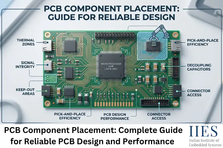
Why Is PCB Component Placement Important?
Component placement is one of the earliest and most critical stages of PCB design. Even a perfect circuit schematic can perform poorly if components are positioned incorrectly.
Benefits of Proper PCB Component Placement
- Improves signal integrity
- Reduces electromagnetic interference (EMI)
- Minimizes crosstalk between high-speed signals
- Simplifies PCB routing
- Improves power distribution
- Reduces voltage drop
- Enhances thermal management
- Makes assembly easier
- Simplifies testing and debugging
- Increases long-term product reliability
Poor Component Placement Can Cause
- Unstable MCU operation
- Communication failures (SPI, I²C, UART, CAN)
- Excessive electrical noise
- Clock instability
- Ground bounce
- Higher power loss
- PCB overheating
- Manufacturing difficulties
- Increased redesign cost

Key PCB Parts and Their Purpose
PCB Part | Purpose |
Substrate | Provides mechanical support |
Copper Layer | Carries electrical signals and power |
Solder Mask | Protects copper from oxidation and short circuits |
Silkscreen | Displays component labels and reference designators |
Vias | Connect traces between PCB layers |
Pads | Allow component soldering |
Traces | Connect electronic components |
Ground Plane | Provides a low-impedance return path |
Power Plane | Distributes supply voltage efficiently |
What Is PCB Layout Design?
PCB layout design is the process of converting an electronic circuit schematic into a physical board by arranging components, routing electrical traces, creating power and ground planes, defining board layers, and preparing manufacturing files.
A successful PCB layout balances electrical performance, thermal behavior, manufacturability, and mechanical constraints.
PCB Layout Design Includes
- Component placement
- PCB footprint selection
- Trace routing
- Power supply design
- Ground plane creation
- Signal integrity optimization
- Impedance control
- Thermal management
- Design Rule Check (DRC)
- Manufacturing file generation (Gerber, Drill Files)
Component placement is completed before most routing begins, making it one of the most influential steps in PCB layout design.
PCB Component Selection
Choosing the right components is just as important as proper PCB component placement. Selecting unsuitable parts can lead to poor performance, overheating, higher power consumption, and manufacturing issues.
Key Selection Criteria
Electrical
- Operating voltage and current
- Power consumption
- Signal frequency
- Tolerance
Mechanical
- Package type
- Board size
- Component height
- Connector placement
Thermal
- Power dissipation
- Junction temperature
- Cooling requirements
Manufacturing
- Package availability
- Assembly compatibility
- Component spacing
- Pick-and-place support
Reliability
- Operating temperature
- Product lifespan
- Environmental conditions
- Moisture sensitivity (MSL)
Always verify component specifications with the manufacturer’s datasheet before finalizing your PCB design.
PCB Component Selection Criteria Checklist
Before finalizing components, verify the following checklist.
Selection Criteria | Why It Matters |
Electrical ratings | Prevents component failure |
Package size | Fits available PCB space |
PCB footprint | Ensures correct assembly |
Availability | Avoids supply chain issues |
Cost | Meets project budget |
Thermal rating | Prevents overheating |
Datasheet specifications | Confirms design compatibility |
Manufacturer support | Improves long-term reliability |
Compliance (RoHS/REACH) | Meets industry standards |
Common PCB Components
- Microcontrollers (STM32, AVR, PIC, ESP32)
- Voltage regulators
- Crystals and oscillators
- Capacitors
- Resistors
- Inductors
- MOSFETs
- Diodes
- Connectors
- Sensors
- Communication ICs
- LEDs
- Switches
- Relays
- Memory ICs
PCB Component Placement
PCB component placement is the foundation of an effective PCB layout. Before routing begins, components should be positioned to minimize signal path lengths, simplify routing, improve heat dissipation, and meet manufacturing requirements.
A good placement strategy reduces design iterations, improves electrical performance, and makes testing and maintenance easier.
Objectives of PCB Component Placement
- Minimize trace lengths
- Reduce signal interference
- Improve signal integrity
- Optimize power distribution
- Simplify PCB routing
- Improve thermal performance
- Support Design for Manufacturing (DFM)
- Reduce production costs
- Improve product reliability
PCB Component Placement Guidelines
Following these guidelines helps improve PCB performance, simplify routing, and support reliable manufacturing.
1. Place Critical Components First
Position key components before placing passive devices.
Examples:
- Microcontrollers and processors
- FPGAs and memory ICs
- Power management ICs
- Connectors
- Crystals and oscillators
2. Group Functional Blocks
Place related components together, such as:
- Power supply
- Analog circuits
- Digital circuits
- RF modules
- Communication interfaces
This reduces routing complexity and electrical noise.
3. Keep Critical Signal Paths Short
Keep connections short between:
- MCU and crystal
- MCU and decoupling capacitors
- Memory devices
- High-speed interfaces
Short traces improve signal integrity and reduce EMI.
4. Maintain Proper Spacing
Provide enough spacing to improve:
- Heat dissipation
- Electrical isolation
- Assembly and inspection
- Rework accessibility
5. Use Consistent Component Orientation
- Align similar components in the same direction.
- Keep polarized components consistent.
- Place connectors for easy access.
- Ensure reference designators remain visible.
6. Design for Manufacturing (DFM)
Verify that the layout supports manufacturing by checking:
- Pick-and-place access
- Soldering clearance
- Test point accessibility
- Component height limits
- Enclosure clearance
PCB Placement Design Rules
Following placement rules reduces design errors and improves board reliability.
Design Rule | Benefit |
Place power circuits near input connectors | Reduces voltage loss |
Keep oscillators close to the MCU | Improves clock stability |
Separate analog and digital sections | Reduces electrical noise |
Place decoupling capacitors close to IC power pins | Improves power stability |
Keep differential pair components together | Maintains signal quality |
Avoid routing under sensitive analog circuits | Reduces interference |
Place heat-generating components away from temperature-sensitive parts | Improves reliability |
Reserve board edges for connectors when possible | Simplifies cable access |
PCB Placement Techniques
Different techniques are used depending on the circuit’s complexity and application.
Functional Placement
Group components according to circuit blocks.
Examples:
- Power supply
- Signal conditioning
- Processing
- Communication
- Output stage
This approach simplifies routing and debugging.
Hierarchical Placement
Begin with the most important components and gradually place supporting devices.
Typical order:
- Connectors
- Power circuitry
- MCU or Processor
- Memory
- Communication ICs
- Passive components
Flow-Based Placement
Arrange components to follow the direction of signal flow.
Example: Sensor → Amplifier → ADC → MCU → Communication Module
This makes the PCB easier to understand and often results in cleaner routing.
Symmetrical Placement
Useful for:
- Differential circuits
- RF layouts
- High-speed communication
- Precision analog circuits
Symmetry helps maintain balanced electrical characteristics.
Signal Integrity and Routing
Good signal integrity ensures signals travel across the PCB without distortion or interference.
Common Issues
- Reflections
- Ringing
- Crosstalk
- Timing errors
- Data corruption
Best Practices
- Keep high-speed traces short.
- Minimize unnecessary vias.
- Maintain continuous ground return paths.
- Route differential pairs together.
- Use 45° bends instead of sharp 90° corners.
- Separate noisy and sensitive signals.
Proper PCB component placement naturally leads to cleaner routing and better signal quality.
Power Distribution and Grounding
A well-designed power and ground network improves circuit stability and reduces electrical noise.
Best Practices
- Use wide traces for high-current paths.
- Keep power loops small.
- Use dedicated power and ground planes in multilayer PCBs.
- Minimize voltage drops.
- Separate analog and digital power when needed.
- Connect decoupling capacitors directly to the ground plane.
A continuous ground plane helps reduce EMI and improves signal integrity.
Impedance Matching
Impedance matching minimizes signal reflections in high-speed PCB designs.
Common Applications
- USB
- Ethernet
- HDMI
- PCIe
- DDR memory
- RF circuits
Best Practices
- Maintain consistent trace width.
- Route differential pairs together.
- Follow the PCB manufacturer’s impedance specifications.
Decoupling Capacitors
Decoupling capacitors stabilize the power supply by filtering high-frequency noise.
Placement Guidelines
- Place capacitors close to IC power pins.
- Keep connections short and wide.
- Use direct ground connections.
- Follow the capacitor recommendations in the component datasheet.
Thermal Management
Proper thermal management improves PCB reliability and extends component life.
Best Practices
- Distribute heat-generating components evenly.
- Keep power devices away from temperature-sensitive parts.
- Use thermal vias, copper pours, or heat sinks where required.
- Provide adequate airflow for high-power designs.
A PCB footprint defines the physical land pattern used to mount a component on the board.
A well-designed footprint ensures reliable solder joints, accurate assembly, and compatibility with manufacturing processes.
- Follow the manufacturer’s recommended land pattern.
- Verify pad dimensions before production.
- Check pin numbering carefully.
- Maintain adequate solder mask clearance.
- Validate footprints using Design Rule Checks (DRC).
Even small footprint errors can lead to assembly failures or difficult rework.
Selecting the correct footprint is just as important as choosing the right component.
Consider These Factors
- Package type (QFN, BGA, SOIC, TQFP, SMD, Through-hole)
- Pin pitch
- Pad dimensions
- Thermal pad requirements
- Assembly method
- Inspection accessibility
Always compare the PCB library footprint with the component datasheet before finalizing the design.
Component Positioning
Effective component positioning balances electrical performance, thermal behavior, mechanical constraints, and manufacturing requirements.
Placement Priorities
- Board connectors
- Power supply section
- Microcontroller or processor
- Clock circuitry
- Memory devices
- Communication interfaces
- Analog circuitry
- Passive components
- Test points
- Mounting holes and mechanical parts
Following a logical placement order simplifies routing, reduces design conflicts, and improves overall PCB quality.

PCB Component Selection Process
Selecting components should involve more than matching values from a schematic. Evaluate electrical, mechanical, thermal, and manufacturing requirements before finalizing parts.
Step 1: Understand the Circuit Requirements
Identify the project’s:
- Operating voltage
- Current consumption
- Signal frequency
- Environmental conditions
- Performance targets
Step 2: Select Suitable Components
Choose components based on:
- Electrical ratings
- Package type
- Availability
- Cost
- Long-term support
Always compare specifications with the manufacturer’s datasheet.
Before PCB layout:
- Match package dimensions
- Verify pin numbering
- Check pad sizes
- Confirm orientation
- Review 3D models if available
Step 4: Review Thermal Requirements
Identify components that generate significant heat. Examples include:
- Voltage regulators
- MOSFETs
- Power ICs
- Motor drivers
- High-power LEDs
Plan adequate spacing and cooling during placement.
Step 5: Validate Before Manufacturing
Perform final checks for:
- Design Rule Check (DRC)
- Electrical Rule Check (ERC)
- Component orientation
- Mechanical clearance
- Assembly compatibility
Choosing the Right PCB Type for Your Project
Selecting the appropriate PCB type depends on the application’s electrical, mechanical, and environmental requirements.
Project Type | Recommended PCB |
Basic learning projects | Single-layer PCB |
Consumer electronics | Double-layer PCB |
Embedded systems | 4-layer PCB |
High-speed communication | Multilayer PCB |
IoT devices | 4 or 6-layer PCB |
Automotive electronics | Multilayer PCB |
Medical devices | Multilayer or Rigid-Flex PCB |
Wearables | Flexible PCB |
LED lighting | Metal-Core PCB |
Selection Factors
- Circuit complexity
- Signal speed
- Power requirements
- Available space
- Cost
- Thermal performance
- Product reliability
Why PCB Design Affects Circuit Performance
PCB performance depends not only on the schematic but also on how components are placed and connected.
A Good PCB Design Improves
- Signal integrity
- Power stability
- EMI performance
- Thermal efficiency
- Mechanical reliability
- Manufacturing quality
- Voltage drops
- Communication failures
- Signal reflections
- Crosstalk
- Excessive heat
- Noise-sensitive analog circuits
- Difficult debugging
- Higher production costs
Proper placement and routing work together to achieve stable and predictable circuit performance.
Common PCB Component Selection Mistakes
Selecting the wrong component can affect performance, reliability, and manufacturability.
Mistake | Impact | How to Avoid It |
Ignoring datasheets | Incorrect operation | Review electrical and mechanical specifications |
Choosing the wrong package | Assembly issues | Verify footprint and package type |
Underrated components | Component failure | Select appropriate voltage and current ratings |
Ignoring thermal limits | Overheating | Check power dissipation and junction temperature |
Selecting obsolete parts | Supply issues | Prefer active and widely available components |
Focusing only on cost | Reduced reliability | Balance price with performance and quality |
PCB Errors and Component Placement Mistakes
Small placement mistakes can significantly affect PCB performance, reliability, and manufacturability. Avoid these common issues:
Decoupling Capacitors Placed Too Far from ICs
Impact: Power supply noise, voltage fluctuations, and unstable MCU operation. Best Practice: Place decoupling capacitors as close as possible to the IC power pins.
Mixing Analog and Digital Circuits
Impact: Noise coupling, reduced ADC accuracy, and signal distortion. Best Practice: Separate analog and digital sections and use proper grounding.
Long Clock Traces
Impact: Clock jitter, timing errors, and increased EMI. Best Practice: Position the crystal oscillator close to the microcontroller.
Poor Connector Placement
Impact: Difficult cable routing, mechanical interference, and assembly issues. Best Practice: Place connectors near the PCB edges while considering enclosure constraints.
Ignoring Heat-Generating Components
Impact: Overheating, reduced reliability, and shorter component lifespan. Best Practice: Distribute heat sources evenly and provide adequate cooling or thermal vias where required.
Best Practices for PCB Component Placement
- Read component datasheets before placement.
- Place critical components first.
- Group related components into functional blocks.
- Keep high-speed signal paths short.
- Use continuous ground planes.
- Place decoupling capacitors close to ICs.
- Keep power loops as small as possible.
- Follow manufacturer-recommended PCB footprints.
- Maintain adequate spacing between components.
- Perform DRC and ERC before manufacturing.
Debugging Tips
Many PCB issues can be identified quickly by following a structured troubleshooting process.
Check | What to Verify | Why It Matters |
Power Supply | Input/output voltage, current consumption, voltage ripple | Ensures stable power and prevents unexpected circuit behavior |
Component Orientation | ICs, electrolytic capacitors, diodes, LEDs, connectors | Incorrect orientation can prevent the board from functioning |
Clock Signals | Oscillator startup, clock frequency, signal stability | An unstable clock can stop the microcontroller from operating correctly |
Solder Joints | Cold joints, solder bridges, missing solder, lifted pads | Poor soldering can cause intermittent or complete circuit failure |
PCB Layout | Ground connections, footprints, routing, shorts, open traces | Identifies layout-related issues that affect circuit performance |

Conclusion
PCB component placement is one of the most important stages of PCB layout design because it directly influences signal integrity, power distribution, thermal performance, manufacturability, and product reliability. A structured placement strategy simplifies routing, reduces design errors, and shortens debugging time.
By following established PCB component placement guidelines, selecting appropriate components and footprints, optimizing power and grounding, and avoiding common placement mistakes, you can design PCBs that perform reliably across embedded systems, IoT devices, industrial controllers, automotive electronics, and other real-world applications. Whether you’re a student or an experienced developer, mastering these fundamentals will help you create more efficient and production-ready PCB designs.