CE Amplifier Characteristics
- Medium-high voltage gain of CE amplifier (50–200 typical)
- Moderate input impedance of CE amplifier
- Moderate output impedance of CE amplifier
- Phase inversion between input and output
- Stable frequency response of CE amplifier
These CE amplifier characteristics make the single stage common emitter amplifier suitable for audio, sensor, and RF circuits.
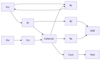
Basic Schematic
2. Circuit Configuration of Single Stage Common Emitter Amplifier
2.1 CE Amplifier Circuit Diagram
The CE amplifier circuit diagram of a single stage common emitter amplifier shows the emitter terminal common to both input and output.
This common emitter amplifier configuration uses a voltage divider bias network, coupling capacitors, and an emitter bypass capacitor to improve gain and stability.
Understanding the CE amplifier circuit diagram is essential to analyze the single stage common emitter amplifier performance.
2.2 Typical Component Values
| Component | Role | Typical Value Range |
|---|
| R1, R2 | Voltage divider | 10kΩ – 100kΩ |
| Rc | Collector resistor | 1kΩ – 10kΩ |
| Re | Emitter resistor | 100Ω – 1kΩ |
| Cin, Cout | Coupling capacitors | 1µF – 10µF |
| Ce | Emitter bypass capacitor | 10µF – 100µF |
The emitter bypass capacitor directly affects the voltage gain of CE amplifier in a single stage common emitter amplifier.

3. DC Biasing Analysis of Single Stage Common Emitter Amplifier
3.1 Voltage Divider Bias CE Amplifier
Vb = Vcc × (R2 / (R1 + R2))
Ve = Vb − Vbe ≈ Vb − 0.7 V
Ie = Ve / Re ≈ Ic
Vce = Vcc − Ic (Rc + Re)
The voltage divider bias CE amplifier method ensures thermal stability and a stable Q-point for the
single stage common emitter amplifier.
3.2 Stability Considerations
Stability Factor (S):
S = (1 + β) / [1 + β (Re / (Re + Rth))]
where,
Rth = R1 || R2
Lower values of S indicate better stability of the single stage common emitter amplifier.
Example Calculation
Vcc = 12 V
R1 = 68 kΩ
R2 = 12 kΩ
Re = 1 kΩ
β = 100
Vb = 12 × (12 / (68 + 12)) = 1.8 V
Ve = 1.8 − 0.7 = 1.1 V
Ie = 1.1 / 1kΩ = 1.1 mA ≈ Ic
Vce = 12 − 1.1 mA × (4.7 kΩ + 1 kΩ) = 5.73 V
S ≈ 7.3

4. AC Small Signal Analysis of Single Stage Common Emitter
Amplifier
4.1 CE Amplifier Small
Parameters
| Parameter | Formula | Typical Value |
|---|
| re | 25 mV / Ie | 5 – 50 Ω |
| gm | Ic / 25 mV | 10 – 100 mS |
| β | ΔIc / ΔIb | 50 – 300 |
| rin | β × re | 500 Ω – 15 kΩ |
4.2 Performance Characteristics
Voltage Gain of CE Amplifier
Without Ce:
Av = − Rc / (re + Re)
With Ce:
Av = − Rc / re
Input Impedance of CE Amplifier
Without Ce:
Zin = R1 || R2 || β (re + Re)
With Ce:
Zin = R1 || R2 || β re
Output Impedance of CE Amplifier
Zout ≈ Rc
5. Frequency Response of Single Stage Common Emitter Amplifier

5.1 Critical Frequency Points
Low-frequency cutoff (Input):
fL ≈ 1 / [2π Cin (Rs + Zin)]
Low-frequency cutoff (Output):
fL ≈ 1 / [2π Cout (Rc + RL)]
High-frequency cutoff:
fH ≈ 1 / [2π (Rc || RL) Cout]
The Miller effect in CE amplifier limits the high-frequency response of the
single stage common emitter amplifier.
5.2 Gain Bandwidth Product of CE Amplifier
GBW = |Av| × BW
BW = fH − fL
6. Practical Design Insight
Designing a single stage common emitter amplifier involves selecting Rc, Re, and bias resistors to meet gain, stability, and bandwidth requirements.
This design methodology is emphasized in hands-on labs at IIES, making it ideal for learners pursuing the
best embedded course in Bangalore.
7. Simulation Results
Input: 10 mVpp @ 1 kHz
Output: 1 Vpp inverted sine wave
Midband gain: 40 dB
Low cutoff: ~80 Hz
High cutoff: ~150 kHz

8. CE Amplifier Applications
- Audio pre-amplifiers
- Sensor interface circuits
- RF IF amplifier stages
Conclusion
The single stage common emitter amplifier remains the most important BJT amplifier because it offers high voltage gain,
stable biasing, and predictable frequency response.
For VTU students, electronics interviews, and embedded careers, mastering the
single stage common emitter amplifier at IIES provides a strong academic and industry advantage through the
best embedded course in Bangalore.