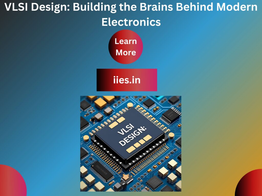
What Is VLSI?
Very Large Scale Integration (VLSI) is the method of merging thousands to billions of transistors into one microchip, referred to as an integrated circuit (IC). These chips are the building blocks of modern electronic devices, handling everything from computation and communication to memory and control—key concepts taught in the best embedded systems course and best IoT course in Bangalore with placement.
VLSI is a step beyond earlier integration scales:
SSI (Small Scale Integration): under 100 transistors
MSI (Medium Scale Integration): 100–1,000 transistors
LSI (Large Scale Integration): 1,000–10,000 transistors
VLSI: more than 10,000 transistors (modern chips have billions!)
Why Is VLSI Important?
Without VLSI, we wouldn’t have the compact, powerful, and affordable devices we rely on today. It enables:
Smaller, faster, and more energy-efficient electronics
High-performance computing (e.g., AI chips, CPUs, GPUs)
Large-scale data storage and memory integration
Advanced tech like IoT, 5G, autonomous vehicles, and robotics
Professionals trained through the best IoT training institute in Bangalore or the best embedded systems course in Bangalore with placement often work directly with VLSI-enabled devices and architectures.
The VLSI Design Process: From Idea to Chip
Designing a VLSI chip is like creating an entire digital ecosystem on a fingernail-sized silicon wafer.
Specification
Define the chip’s functionality, performance, and constraints.
Architecture Design
High-level planning of blocks (e.g., CPU cores, memory, I/O) and their interactions.
RTL Design (Register Transfer Level)
Use HDLs like Verilog or VHDL to describe logic circuits at a functional level—skills emphasized in the best embedded systems and IoT courses.
Functional Verification
Simulate RTL code to validate logical accuracy.
Synthesis
Convert RTL code into gate-level netlists using standard logic gates.
Physical Design
Implement the logical design onto silicon with:
Fabrication
Manufacture the final chip on silicon wafers using semiconductor fabrication techniques.
Testing and Packaging
Perform defect testing and integrate the chip into devices.
Tools of the Trade
Modern VLSI designers use sophisticated software tools taught in the best embedded systems course:
Applications of VLSI
| Field | Example Applications |
|---|
| Consumer Electronics | Smartphones, smartwatches, laptops |
| Automotive | Advanced driver-assistance systems (ADAS) |
| Telecommunications | 5G modems, signal processors |
| Healthcare | Wearable health monitors, pacemakers |
| Aerospace & Defense | Radar, GPS, secure communication systems |
| AI & ML | Neural network accelerators (e.g., TPUs) |
VLSI plays a key role in sectors often explored in top-rated IoT training with placement programs.
Challenges in VLSI Design
Despite its benefits, VLSI design presents several challenges:
Power Consumption: Crucial for mobile and wearable devices
Complexity: Increases with billions of transistors
Fabrication Cost: Requires expensive cleanroom environments
Miniaturization Constraints: Physical limits of Moore’s Law are approaching
Future of VLSI
The field of VLSI is evolving with groundbreaking developments:
3D ICs: Stacking chips vertically
SoCs (System on Chip): Integrating multiple functions onto one chip
AI Chips: Tailored for deep learning and neural networks
Quantum and Neuromorphic VLSI: Next-gen computing technologies
Courses at the best IoT course in Bangalore with placement frequently touch on these trends to prepare students for future industry roles.
Final Thoughts
VLSI design is the invisible powerhouse behind the technological transformation of our century. From the processors in laptops to the advanced chips in Mars rovers, it’s about integrating greater power into smaller spaces. Whether you’re curious about what powers your smartphone or pursuing the best embedded systems course or best IoT course to launch your tech career, mastering VLSI opens doors to a future in electronics and intelligent systems.
At the Indian Institute of Embedded Systems (IIES), we equip students with in-demand skills in VLSI, embedded systems, and IoT through practical, placement-focused training. If you’re seeking the best IoT training institute in Bangalore or the best embedded systems course in Bangalore with placement, IIES is your gateway to cutting-edge careers in core technology domains.