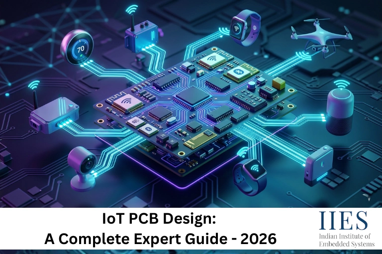
What is PCB Design in IoT?
PCB design in IoT refers to the process of creating a printed circuit board that connects and supports all electronic components used in an IoT device, such as sensors, microcontrollers, communication modules, and power systems.
A typical IoT PCB includes:
- Microcontroller or processor
- Wireless communication module (WiFi/Bluetooth/LoRa)
- Sensors (temperature, motion, humidity, etc.)
- Power management system
- Antenna system
Unlike traditional electronics, IoT systems require:
- Low power consumption
- Compact design
- Wireless connectivity
- High reliability in real-world environments
This combination makes IoT PCB design more complex but also more interesting.

PCB Full Form in IoT (and Why It Matters)
The PCB full form in IoT is Printed Circuit Board. It is the physical platform that connects electronic components using copper tracks.
In IoT systems, PCBs are not just connectors, they are the brain-to-hardware interface that ensures seamless communication between sensors and cloud systems.
Without PCB design:
- Devices would be bulky
- Connections would be unreliable
- Power efficiency would drop significantly
PCB in IoT: The Core of Smart Devices
When we talk about PCB in IoT, we are referring to the backbone that enables:
- Data collection from sensors
- Wireless data transmission
- Real-time processing
- Cloud communication
For example:
A smart agriculture sensor node uses a PCB to:
- Read soil moisture data
- Process it using a microcontroller
- Send it via LoRa or WiFi to a cloud dashboard
This is why PCB design for IoT is considered one of the most critical skills in embedded systems engineering today.
Traditional PCB vs IoT PCB Design: Key Differences
Understanding the difference between traditional PCB design and IoT PCB design helps highlight why IoT hardware requires specialized approaches.
Feature | Traditional PCB | PCB Design in IoT |
Power Usage | High | Ultra-low (battery optimized) |
Connectivity | Limited (wired) | Wireless (WiFi, Bluetooth, LoRa) |
Size | Larger boards | Compact and miniaturized |
Complexity | Moderate | High (multi-functional integration) |
Optimization Focus | Basic functionality | Power efficiency + connectivity |
Scalability | Limited | Designed for large-scale deployments |
In the modern world engineers must balance power consumption, wireless performance, and compact design, making IoT PCB development significantly more advanced than traditional PCB design.
PCB Design Process in IoT (Step-by-Step Workflow)
A structured PCB design process in IoT ensures reliability and scalability.
1. Requirement Analysis
Define:
- Power constraints
- Communication method
- Sensor types
- Size limitations
2. Component Selection
Choose:
- Microcontrollers (ESP32, STM32, etc.)
- Sensors
- Power ICs
- Wireless modules
3. Schematic Design
Create circuit connections using CAD tools.
Focus on:
- Component placement
- Signal routing
- Ground planes
- EMI reduction
5. Validation
Run:
- Design Rule Check (DRC)
- Electrical Rule Check (ERC)
6. Prototyping
Fabricate and test real-world performance.
7. Iteration
Improve based on thermal, power, or signal issues.
PCB Design in IoT Checklist for Reliable Hardware
Before finalizing your IoT PCB design, it is essential to verify that all critical aspects of the board are optimized for performance, efficiency, and reliability. This checklist provides a structured approach to ensure your design is ready for real-world deployment.
Power and Efficiency
- Ensure the power supply is stable and properly regulated
- Select low-power components for battery-operated devices
- Implement sleep modes and power-saving strategies
Connectivity and RF Design
- Optimize antenna placement and isolate it from interference sources
- Keep RF traces short and ensure proper impedance matching
- Position wireless modules to maximize signal strength
Signal Integrity
- Minimize the length of high-speed signal traces
- Maintain proper grounding and return paths
- Place decoupling capacitors close to IC power pins
Thermal Management
- Provide adequate spacing for heat-generating components
- Use thermal vias or copper pours for heat dissipation
- Avoid thermal hotspots in compact layouts
Layout and Component Placement
- Separate analog and digital sections of the circuit
- Group components based on functionality
- Avoid overcrowding that complicates routing and airflow
Design Validation
- Perform Design Rule Check (DRC)
- Verify Electrical Rule Check (ERC)
- Test prototypes under real operating conditions
PCB Design Workflow (Industry Standard)
A typical PCB design workflow in IoT development looks like this:
Requirement → Schematic → Simulation → Layout → Review → Fabrication → Testing → Optimization
Each stage directly impacts:
- Performance
- Cost
- Scalability
PCB Layout Best Practices for IoT Systems
Strong PCB layout best practices ensure long-term device stability.
Key practices include:
- Keep high-speed traces short
- Use ground planes for noise reduction
- Place decoupling capacitors near ICs
- Separate analog and digital sections
- Avoid sharp 90° trace angles
- Optimize antenna placement
- Ensure proper thermal dissipation
These practices significantly improve signal integrity and power efficiency.

IoT PCB Architecture Explained (Layer-by-Layer)
A well-optimized PCB design for iot is not just about placing components, it’s about structuring the board in layers to ensure signal integrity, power efficiency, and reliable wireless communication.
A typical IoT PCB board architecture includes:
- Power Layer
Distributes stable voltage across the board. Proper design here reduces noise and improves battery efficiency. - Ground Layer
Acts as a reference plane for all signals. A solid ground plane minimizes EMI and improves overall signal stability. - RF Layer (Wireless Section)
Dedicated to communication modules like WiFi, Bluetooth, or LoRa. This layer requires careful routing and isolation to prevent signal loss. - Sensor Interface Layer
Connects sensors and analog components. Proper separation from digital circuits helps reduce interference and ensures accurate readings.
In advanced designing printed circuit boards in IoT, multi-layer PCBs (4-layer or more) are commonly used to separate these functions efficiently, leading to better performance in compact devices.
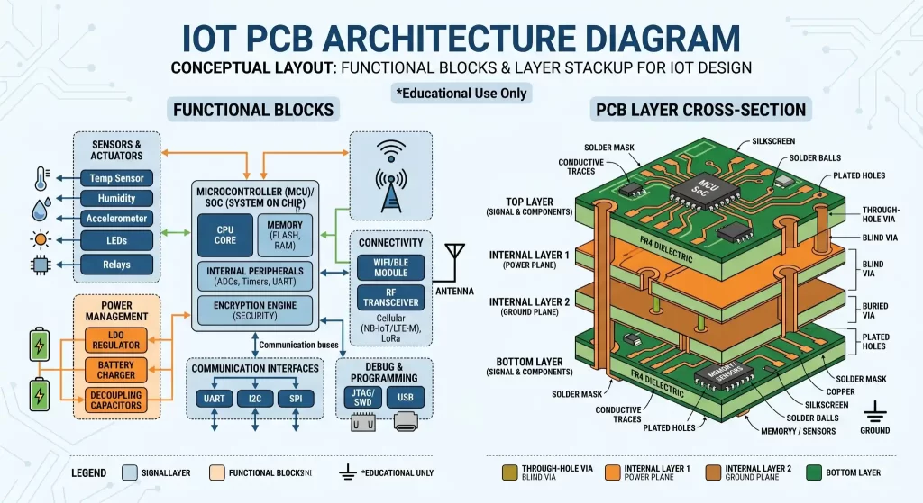
Detailed IoT PCB architecture showing MCU, sensors, RF communication modules, power management, and a multi-layer PCB stack (signal, power, and ground planes).
Common Failures (And How to Avoid Them)
Even well-planned PCB design projects can fail due to small but critical mistakes. Identifying these issues early can save time, cost, and product reliability.
Here are some of the most common failures:
- Poor Antenna Grounding
Leads to weak or unstable wireless signals. Always ensure proper grounding and keep the antenna area free from interference. - Overheating in Compact Designs
Tight layouts without proper thermal management can cause component failure. Use thermal vias, copper pours, and proper spacing. - Battery Drain Issues
Inefficient power design or improper sleep mode configuration can drastically reduce battery life in IoT devices. - EMI Interference
Poor routing and lack of shielding can introduce noise, affecting signal integrity and communication reliability. - Improper Component Placement
Placing sensitive analog components near noisy digital circuits can lead to inaccurate sensor readings.
Quick Tip:
A robust PCB design workflow should always include simulation and real-world testing to catch these failures before production.
Best PCB Design Software (2026)
Choosing the right tools improves productivity and accuracy.
Popular tools include:
- Altium Designer
- KiCad
- EasyEDA
- Autodesk EAGLE
These tools support:
- Schematic capture
- 3D visualization
- Simulation
- Manufacturing export
IoT Sensor Node PCB Design (Real-World Example)
A practical example of iot sensor node pcb design:
Scenario:
A smart environmental monitoring system.
PCB Includes:
- Temperature sensor
- Humidity sensor
- ESP32 microcontroller
- LoRa module
- Lithium battery management system
Key design focus:
- Ultra-low power consumption
- Sleep mode optimization
- Compact PCB footprint
- Stable wireless communication
This type of design is widely used in:
- Smart agriculture
- Industrial monitoring
- Smart cities
Scaling Up Software in IoT Systems
While hardware is critical, scaling up software in IoT is equally important.
Key challenges include:
- Device communication management
- Cloud integration
- Firmware updates (OTA)
- Data synchronization
A well-designed PCB supports scalable software by ensuring:
- Stable communication interfaces
- Reliable power delivery
- Minimal hardware bottlenecks
IoT PCB Board: Design Considerations
An iot pcb board must balance:
Electrical factors:
- Signal integrity
- EMI shielding
- Power efficiency
Physical factors:
- Size constraints
- Heat dissipation
- Durability
Connectivity factors:
- Wireless antenna performance
- Protocol compatibility
What Are the Components of IoT?
A typical IoT system includes:
- Sensors
- Microcontrollers
- Communication modules
- Power systems
- Cloud integration layer
Each component must be carefully placed during PCB design for optimal performance.
PCB Design Ideas for IoT Projects
If you are building projects, here are ideas:
- Smart home automation board
- Air quality monitoring system
- Smart irrigation controller
- Wearable health tracker PCB
- Industrial machine monitoring board
Common Mistakes
Avoid these errors:
- Poor antenna placement
- Ignoring thermal design
- Overcrowding components
- Weak power regulation design
- Not testing EMI/EMC issues
These mistakes often lead to unstable IoT devices.

Future Trends in IoT PCB Design (2026 and Beyond)
- AI-assisted PCB layout optimization
- Ultra-low power energy harvesting boards
- Flexible and wearable PCBs
- RISC-V based IoT hardware
- Edge AI integrated PCBs
This shift is making IoT hardware smarter and more efficient.
Conclusion
IoT PCB design is the foundation of every modern connected device. From simple sensor nodes to complex industrial systems, the quality of PCB design determines performance, reliability, and scalability.
By understanding the PCB design process in IoT, following best layout practices, and using the right tools, engineers can build efficient and future-ready IoT systems.
As IoT continues to evolve, mastering designing printed circuit boards will remain one of the most valuable skills in embedded engineering.