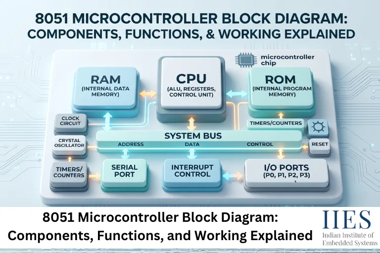
What Is the 8051 Microcontroller Block Diagram?
The 8051 microcontroller block diagram is a simplified representation of the internal hardware organization of the 8051 microcontroller.
It shows how different hardware blocks are connected and how they exchange data during program execution.
The block diagram helps explain:
- How instructions are executed
- How data moves inside the microcontroller
- How memory is accessed
- How peripherals communicate with the CPU
- How external devices are controlled
Unlike a circuit diagram, the block diagram focuses on the functionality of each module rather than the electrical connections.

Complete 8051 Microcontroller Block Diagram
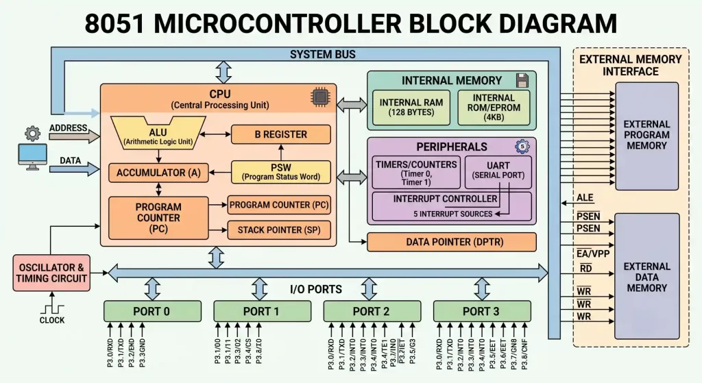
Internal architecture and key peripheral components of the 8051 Microcontroller.
Main Components of the 8051 Microcontroller Block Diagram
The standard 8051 functional block diagram consists of the following major hardware modules.
Component | Function |
CPU | Executes program instructions |
ALU | Performs arithmetic and logical operations |
Accumulator | Stores operands and ALU results |
Register Bank | Holds temporary working registers |
Program Counter | Points to the next instruction |
Stack Pointer | Manages stack operations |
Internal RAM | Stores variables and temporary data |
Program Memory | Stores firmware or program code |
Timers and Counters | Generates delays and counts events |
UART | Enables serial communication |
Interrupt Controller | Handles interrupt requests |
I/O Ports | Interfaces with external hardware |
Oscillator | Provides the system clock |
External Memory Interface | Connects external memory devices |
Each block has a dedicated role in executing embedded applications efficiently.
CPU (Central Processing Unit)
The CPU is the control center of the 8051 microcontroller.
It executes program instructions stored in program memory and coordinates communication between all internal modules.
Primary Responsibilities
- Fetches instructions
- Decodes instructions
- Executes operations
- Controls data movement
- Coordinates memory access
- Communicates with peripherals
Without the CPU, the remaining hardware blocks cannot function together.
Arithmetic Logic Unit (ALU)
The 8051 ALU performs arithmetic and logical operations on data.
It receives operands from registers or memory, processes them, and stores the result in the accumulator or another destination register.
Arithmetic Operations
- Addition
- Subtraction
- Increment
- Decrement
- Multiplication
- Division
Logical Operations
- AND
- OR
- XOR
- NOT
- Compare
- Rotate
- Shift operations
The ALU also updates status flags such as Carry and Overflow after many operations.
Accumulator in 8051
The Accumulator (Register A) is one of the most frequently used registers in the 8051 microcontroller.
Most arithmetic, logical, and data transfer instructions use the accumulator as the default register.
Functions of the Accumulator
- Stores ALU operands
- Holds calculation results
- Transfers data
- Performs logical operations
- Supports bit manipulation
Example
MOV A,#25H

ADD A,#10H
In this example:
- The value 25H is loaded into the accumulator.
- The ALU adds 10H.
- The final result is stored back in Register A.
Register Bank in 8051
The Register Bank contains four groups of general-purpose registers.
Each bank has eight registers: R0, R1, R2, R3, R4, R5, R6, R7.
Since there are four register banks, the 8051 provides a total of 32 register locations.
Register Bank | Address Range |
Bank 0 | 00H–07H |
Bank 1 | 08H–0FH |
Bank 2 | 10H–17H |
Bank 3 | 18H–1FH |
Why Multiple Register Banks?
Multiple register banks reduce memory access time and allow faster context switching during interrupt handling.
Program Counter in 8051
The Program Counter (PC) is a 16-bit register that stores the address of the next instruction to be executed.
Every time an instruction is fetched, the program counter updates automatically.
Functions
- Points to the next instruction
- Controls program sequence
- Supports jumps and branches
- Works with call and return instructions
Example
If the current instruction is stored at address 0100H, the Program Counter updates to the next instruction unless a branch or jump changes the execution flow.
Stack Pointer in 8051
The Stack Pointer (SP) manages the stack area in internal RAM.
The stack temporarily stores important information during program execution.
Stack Stores
- Return addresses
- Register values
- Temporary variables
- Interrupt information
Common Stack Operations
By default, the Stack Pointer starts at 07H, meaning the first pushed value is stored at 08H.
Proper stack management helps prevent data corruption, especially in applications that use nested function calls or multiple interrupts.
Internal RAM in 8051
The standard 8051 microcontroller includes 128 bytes of internal RAM, which stores temporary data during program execution.
The RAM is divided into different sections for specific purposes.
Memory Area | Purpose |
Register Banks | General-purpose registers |
Bit-Addressable Area | Individual bit operations |
General-Purpose RAM | Variables and temporary data |
Internal RAM offers much faster access than external memory, making it suitable for frequently used variables and intermediate results.
Program Memory in 8051
Program Memory stores the firmware or machine code that the CPU executes. Unlike RAM, program memory is non-volatile, meaning the code remains stored even after power is turned off.
In the original 8051 microcontroller:
- 4 KB on-chip ROM
- Stores application program
- Accessed by the Program Counter
- Can use external program memory if required
Functions of Program Memory
- Stores executable instructions
- Holds lookup tables and constant data
- Provides instructions to the CPU during execution
- Supports larger applications using external ROM
Program Memory vs Data Memory
Feature | Program Memory | Data Memory |
Purpose | Stores program code | Stores variables and data |
Volatility | Non-volatile | Volatile |
Access | CPU instruction fetch | Read/Write operations |
Default Size (8051) | 4 KB ROM | 128 Bytes RAM |
Data Memory in 8051
Data Memory stores information that changes while the program is running.
Unlike program memory, its contents are lost when power is removed.
Data memory is used for:
- Variables
- Temporary calculations
- Sensor values
- Flags
- Buffers
- Stack data
The CPU continuously reads from and writes to data memory during program execution.
Control Unit in 8051
The Control Unit (CU) manages and coordinates all operations inside the microcontroller. It does not perform calculations itself but directs other hardware blocks to execute instructions in the correct sequence.
Functions of the Control Unit
- Fetches instructions from program memory
- Decodes machine instructions
- Generates internal control signals
- Controls data transfer between modules
- Synchronizes CPU operations
- Coordinates memory and peripheral access
How the Control Unit Works
- Fetches the next instruction using the Program Counter.
- Decodes the instruction opcode.
- Activates the required hardware blocks.
- Executes the instruction.
- Updates the Program Counter for the next instruction.
Without the Control Unit, the CPU cannot coordinate the activities of the ALU, memory, registers, or peripherals.
Timers and Counters in 8051
The Timers and Counters generate precise delays, measure time intervals, and count external events.
The standard 8051 includes Timer 0 and Timer 1. Each timer is 16-bit and can operate as either Timer mode or Counter mode.
Timer Mode
Used for measuring internal clock cycles.
Typical applications include:
- Software delays
- Periodic interrupts
- PWM generation (software-based)
- Task scheduling
Counter Mode
Counts external pulses received on dedicated pins.
Typical applications include:
- Object counting
- Pulse counting
- Frequency measurement
- Encoder input
Timer Applications
Application | Purpose |
LED blinking | Delay generation |
Digital clock | Time keeping |
PWM | Motor speed control |
Frequency measurement | Count incoming pulses |
Industrial automation | Event counting |
The UART (Universal Asynchronous Receiver/Transmitter) enables serial communication between the 8051 microcontroller and external devices.
Common communication partners include computers, GPS modules, GSM modules, Bluetooth modules, Wi-Fi modules, and other microcontrollers.
The UART converts parallel data into serial data during transmission and serial data back into parallel form during reception.
UART Functions
- Serial data transmission
- Serial data reception
- Baud rate control
- Full-duplex communication
Common Applications
- Debugging using serial terminal
- Sensor communication
- Wireless modules
- Embedded monitoring systems
Interrupt System in 8051
The Interrupt System allows the microcontroller to respond immediately to important events without continuously checking their status.
Instead of waiting inside a polling loop, the CPU temporarily pauses the current task, executes an Interrupt Service Routine (ISR), and then resumes the interrupted program.
Standard Interrupt Sources
Interrupt | Purpose |
External Interrupt 0 | External event detection |
Timer 0 Overflow | Timer interrupt |
External Interrupt 1 | External event detection |
Timer 1 Overflow | Timer interrupt |
Serial Port Interrupt | UART communication |
Advantages of Interrupts
- Faster response to external events
- Reduces CPU workload
- Improves overall system efficiency
- Supports real-time embedded applications
Oscillator and Clock Circuit
Every operation inside the 8051 microcontroller depends on a clock signal generated by the Oscillator Circuit.
The oscillator determines how quickly instructions are executed and how peripherals such as timers and serial communication operate.
The classic 8051 commonly uses an 11.0592 MHz crystal or a 12 MHz crystal. The 11.0592 MHz crystal is especially popular because it allows accurate standard UART baud rates with minimal error.
Functions of the Oscillator
- Generates the system clock
- Synchronizes all internal operations
- Controls instruction execution speed
- Drives timers and UART timing
8051 I/O Ports
The standard 8051 provides 32 programmable input/output pins, organized into four 8-bit ports.
Port | Pins | Primary Function |
Port 0 | P0.0–P0.7 | General I/O and external memory interface |
Port 1 | P1.0–P1.7 | General-purpose I/O |
Port 2 | P2.0–P2.7 | General I/O and higher address bus |
Port 3 | P3.0–P3.7 | I/O with alternate peripheral functions |
Common Uses of I/O Ports
- Reading switches
- Controlling LEDs
- Driving LCD displays
- Interfacing keypads
- Reading sensors
- Controlling relays
- Motor interfacing
Port 3 also supports dedicated functions such as UART communication, interrupts, timer inputs, and external memory control.
External Memory Interface in 8051
The External Memory Interface allows the 8051 to expand beyond its built-in memory by connecting external ROM or RAM.
This feature is useful for applications requiring larger firmware, more data storage, or complex embedded programs.
External Memory Features
- Supports external program memory
- Supports external data memory
- Uses multiplexed address and data bus
- Controlled using dedicated control signals
Important Signals
Signal | Function |
ALE | Address Latch Enable |
PSEN | Program Store Enable |
RD | External Data Read |
WR | External Data Write |
This interface increases system flexibility, allowing developers to build applications that exceed the internal memory capacity of the standard 8051.

How Does the 8051 Microcontroller Block Diagram Work?
The functional blocks of the 8051 operate together in a coordinated sequence to execute a program.
Step 1: Fetch Instruction
The Program Counter points to the next instruction. The instruction is fetched from Program Memory.
Step 2: Decode Instruction
The Control Unit decodes the instruction. It determines which hardware blocks are required.
Step 3: Process Data
Required data is read from Registers or Internal RAM. The ALU performs arithmetic or logical operations. Results are stored in the Accumulator or memory.
Step 4: Access Peripherals
Depending on the instruction, the CPU may:
- Read an input from an I/O port
- Send data through UART
- Start a timer
- Handle an interrupt
- Access external memory
Step 5: Execute Next Instruction
The Program Counter updates automatically. The CPU repeats the cycle until the program finishes or resets.
How the Functional Blocks Work Together
Block | Role During Execution |
Program Counter | Locates the next instruction |
Program Memory | Stores executable code |
Control Unit | Decodes instructions and coordinates hardware |
ALU | Performs calculations and logical operations |
Accumulator | Holds operands and computation results |
Register Bank | Stores temporary working data |
Internal RAM | Holds variables and stack data |
Timers | Generate delays and measure time |
UART | Enables serial communication |
I/O Ports | Connect the microcontroller to external devices |
Oscillator | Provides the clock for synchronized operation |
External Memory Interface | Expands memory when internal storage is insufficient |
This coordinated operation enables the 8051 microcontroller to execute embedded applications efficiently, from simple LED blinking programs to communication, automation, and control systems.
Key Features of the 8051 Microcontroller Block Diagram
The 8051 functional block diagram combines several hardware modules that work together to execute embedded applications efficiently.
Major Features
- 8-bit CPU architecture
- Built-in Arithmetic Logic Unit (ALU)
- Four register banks with eight registers each
- 16-bit Program Counter
- 8-bit Stack Pointer
- 128 bytes of internal RAM
- 4 KB on-chip program memory (standard 8051)
- Two 16-bit Timers/Counters
- Full-duplex UART for serial communication
- Five interrupt sources with two priority levels
- Four 8-bit programmable I/O ports (32 I/O pins)
- External memory expansion support
- On-chip oscillator and clock circuit
These integrated hardware blocks make the 8051 suitable for a wide range of embedded control and monitoring tasks.
Advantages of the 8051 Microcontroller Block Diagram
Understanding the 8051 microcontroller block diagram provides a strong foundation for learning embedded systems and firmware development.
Some of its key advantages include:
- Simple and easy-to-understand architecture
- Clearly separated functional modules
- Efficient instruction execution through dedicated hardware blocks
- Built-in peripherals reduce external component requirements
- Supports both internal and external memory
- Reliable interrupt handling for event-driven applications
- Suitable for learning microcontroller fundamentals
- Large ecosystem of documentation, examples, and development tools
Limitations of the 8051 Microcontroller Block Diagram
Although the 8051 remains an excellent educational microcontroller, its hardware capabilities are limited compared to modern 32-bit microcontrollers.
- Limited internal RAM (128 bytes in the standard 8051)
- Lower processing speed than modern microcontrollers
- No built-in ADC or DAC
- Limited program memory
- Restricted peripheral integration
- Not suitable for high-performance embedded applications such as machine vision or Edge AI
Modern embedded systems often require faster processors, larger memory, and advanced peripherals that extend beyond the capabilities of the classic 8051.
8051 Block Diagram vs Modern Microcontrollers
Feature | 8051 | Modern ARM Cortex-M MCU |
CPU | 8-bit | 32-bit |
Internal RAM | 128 Bytes | Several KB to MB |
Program Memory | 4 KB ROM | Flash memory up to several MB |
Clock Speed | Typically up to 12–33 MHz | 48 MHz to several hundred MHz |
Timers | 2 | Multiple advanced timers |
Communication | UART | UART, SPI, I²C, CAN, USB, Ethernet and more |
ADC/DAC | Not available (standard 8051) | Commonly integrated |
Performance | Basic control applications | Complex embedded applications |
While the 8051 is still widely used for education and simple control systems, modern microcontrollers offer greater performance, memory capacity, and peripheral integration for advanced embedded designs.
Conclusion
The 8051 microcontroller block diagram provides a clear view of how the internal hardware modules cooperate to execute embedded programs. Each component, including the CPU, ALU, accumulator, register banks, program counter, stack pointer, memory, timers, UART, I/O ports, control unit, and oscillator, has a specific role in processing instructions and controlling external devices.
Rather than viewing these modules independently, it is important to understand how they interact during the instruction execution cycle. This understanding simplifies firmware development, hardware interfacing, debugging, and system design while strengthening the fundamentals required for learning modern microcontrollers.
Whether you are studying embedded systems, preparing for technical interviews, or beginning microcontroller programming, a solid understanding of the 8051 functional block diagram forms an essential foundation for embedded engineering.