1. Overview of CMOS Technology
CMOS technology (Complementary Metal-Oxide-Semiconductor) is the foundation of all modern digital ICs. In CMOS technology, NMOS and PMOS transistors work together in a complementary way to form logic circuits. Almost every microcontroller, processor, memory IC and system-on-chip today is fabricated using CMOS technology.
Why CMOS Technology?
- Extremely low static power consumption
- High immunity to noise due to large CMOS noise margin
- High integration density enabling CMOS in VLSI
- Excellent scalability for advanced fabrication nodes
These CMOS technology advantages make it the dominant semiconductor process.
2. MOSFET Fundamentals
| Terminal | Name |
|---|
| G | Gate |
| D | Drain |
| S | Source |
| B | Body / Substrate |
The gate voltage controls MOSFET channel formation. When the gate exceeds the threshold voltage in MOSFET, a conductive channel forms between source and drain.

3. NMOS and PMOS Operation
NMOS Transistor Working
- Built on p-type substrate
- n+ source and drain regions
- Conducts when gate is HIGH
- Forms the NMOS pull-down network
PMOS Transistor Working
- Built in n-well
- p+ source and drain regions
- Conducts when gate is LOW
- Forms the PMOS pull-up network
This complementary behavior is called NMOS and PMOS operation, the heart of CMOS technology.
4. CMOS Inverter – CMOS Logic Inverter
The CMOS inverter (also called CMOS logic inverter) is the simplest CMOS gate.
CMOS Inverter Diagram
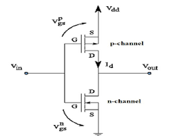
Structure
- PMOS on top connected to VDD
- NMOS at bottom connected to GND
- Gates tied together as input
- Drains connected as output
CMOS Inverter Operation
| Input | PMOS | NMOS | Output |
|---|
| 0 | ON | OFF | 1 (VDD) |
| 1 | OFF | ON | 0 (GND) |
CMOS Inverter Characteristics
- High voltage gain
- Sharp switching region
- Large CMOS noise margin
- Very low power dissipation
CMOS Inverter VTC Curve

The CMOS inverter VTC curve plots output voltage versus input voltage and shows a steep transition, proving the reliability of CMOS technology.

5. Power Consumption in CMOS
Static Power
Ideally zero because there is no DC path between VDD and GND in steady state.
CMOS Dynamic Power Equation
P = α × CL × VDD2 × f
Where: α = switching activity factor, CL = load capacitance in CMOS, f = operating frequency.
6. CMOS Gates – CMOS AND Gate & XOR Gate with CMOS
- A CMOS gate is created using pull-up and pull-down networks.
- CMOS AND gate is built using NAND + inverter.
- XOR gate with CMOS uses complex NMOS–PMOS networks.
- Every AND CMOS circuit in processors is built using CMOS technology.
7. CCD v CMOS
| Feature | CCD | CMOS |
|---|
| Fabrication | Special process | Standard CMOS technology |
| Power | High | Very low |
| Speed | Slower | Faster |
| Integration | External ADC | On-chip ADC using CMOS in VLSI |
| Mobile usage | Rare | CMOS sensor in mobile phones |
8. CMOS in VLSI – Real-Time Applications
- Microcontrollers (Arduino, STM32, ESP32)
- Smartphone processors and CMOS sensor in mobile cameras
- Automotive ECUs
- Medical wearable electronics
- IoT and networking routers
9. Summary Table – NMOS vs PMOS
| Feature | NMOS | PMOS |
|---|
| Charge carriers | Electrons | Holes |
| Gate condition | HIGH | LOW |
| Network role | Pull-down | Pull-up |
| Connected to | GND | VDD |
| Speed | Faster | Slightly slower |
10. Career Scope – Learn CMOS Technology at IIES Bangalore
To master CMOS technology, join the best embedded course in Bangalore – IIES. IIES also provides the best VLSI internship in Bangalore, covering CMOS inverter design, CMOS gate implementation, CMOS in VLSI chip flow, and practical CMOS simulation projects.
Conclusion
From CMOS inverter, CMOS gate, CMOS logic inverter, XOR gate with CMOS, to camera applications like CMOS sensor in mobile, everything today depends on CMOS technology. Whether it is CCD v CMOS comparison or designing chips using CMOS in VLSI, the foundation always remains CMOS technology.