Printed Circuit Board Design Basics: From Design to Final Artwork

Printed Circuit Board Design

INTRODUCTION

 Printed Circuit Boards (PCBs) are the unsung heroes of modern electronics, providing a robust and organized platform for connecting various electronic components. 

From the initial design phase to the creation of the final artwork, the journey of a PCB involves meticulous planning and execution.

 This article aims to unravel the intricacies of PCBs, exploring the key stages from design conception to the generation of final artwork.

Design Phase: The Blueprint of Innovation

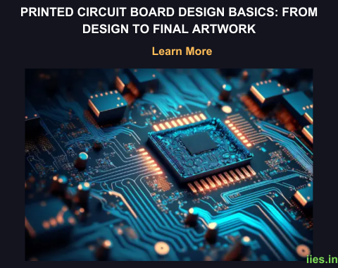
The journey begins with the design phase, where the blueprint of the electronic device comes to life. PCB design involves arranging electronic components and creating interconnections using a design software. This phase requires a deep understanding of circuitry, electrical engineering principles, and the intended functionality of the device. Designers use specialized software tools like Altium, Eagle, or KiCad to create a virtual representation of the PCB layout. During the design phase, considerations such as component placement, signal routing, and power distribution are crucial. The efficiency and reliability of the final PCB depend on the effectiveness of these choices. Designers must also account for factors like signal integrity, thermal management, and manufacturability to ensure the end product meets its performance requirements.

Schematic Capture: Building the Logical Framework

Once the initial design is conceptualized, the schematic capture phase begins. This involves creating a graphical representation of the circuit using symbols to represent components and lines to denote connections. The schematic serves as a blueprint for the PCB layout and guides the designer in placing components and routing traces. The schematic capture phase is critical for ensuring the logical integrity of the circuit. It helps designers identify potential issues and optimize the design before moving on to the physical layout. This phase involves collaborative efforts between electrical engineers and PCB designers to refine the circuitry and eliminate potential errors.

PCB Design Layout: Translating Concept to Reality

With the schematic in hand, the focus shifts to the PCB Design layout, where the virtual design is translated into a physical form. During this phase, designers place components on the board, define their connections, and route the traces that carry electrical signals. The goal is to create an organized and compact layout that minimizes signal interference and ensures optimal performance. Advanced PCB layout tools enable designers to implement various design rules, such as minimum trace widths, clearance between traces, and layer stackup configurations. These rules help maintain signal integrity, prevent crosstalk, and ensure the manufacturability of the final board.

Component Footprints: Precision in Placement

The accuracy of component placement is crucial for the functionality and reliability of the PCB. Each electronic component has a specific footprint, which includes the arrangement of pins or pads for soldering. Designers must select or create accurate component footprints to ensure proper alignment and connectivity. Modern PCB design software often comes with a library of predefined component footprints, but customization may be required for unique components. Accurate placement of components is essential to meet electrical and mechanical specifications, and designers must carefully review the layout to identify any potential issues.

Routing: Tracing the Path to Connectivity

Routing involves creating the paths (traces) that connect the various components on the PCB. This phase demands a delicate balance between achieving an efficient layout and adhering to design rules. Designers must consider factors such as signal integrity, impedance matching, and minimizing electromagnetic interference during the routing process. The complexity of routing increases with the density of components and the number of layers in the PCB. Multilayer PCBs offer more routing flexibility, allowing designers to create intricate layouts while maintaining signal integrity. Automated routing tools assist designers in optimizing trace routes and meeting design specifications.

Design Validation: Ensuring Reliability

Before proceeding to the manufacturing phase, thorough design validation is essential to identify and rectify any potential issues. Simulation tools can be employed to analyze the behavior of the circuit, ensuring that the design meets performance requirements. This phase helps catch errors, validate signal integrity, and optimize the design for reliability.

Generating Gerber Files: The Language of Manufacturing

Once the design is validated, the next step is to generate Gerber files, which serve as the universal language for PCB Design manufacturing. Gerber files contain information about the PCB layers, component placement, and copper traces. These files are crucial for the fabrication and assembly processes, providing manufacturers with the necessary instructions to bring the design to life.

Manufacturing: Bringing the Design to Reality

With Gerber files in hand, the manufacturing phase begins. The PCB fabrication process involves the creation of the actual board using materials like fiberglass and copper. The Gerber files guide the etching of copper layers, drilling of holes, and application of solder mask and silkscreen. After fabrication, the PCB moves to the assembly phase, where electronic components are soldered onto the board. Automated pick-and-place machines precisely position components, and reflow soldering ensures secure connections. Thorough quality control measures are implemented to identify and rectify any manufacturing defects.

Testing and Debugging: Ensuring Functionality

Once the PCB is assembled, thorough testing and debugging are conducted to ensure that the final product functions as intended. Various testing methods, such as functional testing, in- circuit testing, and boundary scan testing, are employed to verify the electrical and functional performance of the PCB. Any issues identified during testing are addressed through redesign or component replacement.

Conclusion: The Artistry of Connectivity

In conclusion, the journey from PCB design to final artwork is a meticulous and multifaceted process that demands expertise, precision, and a deep understanding of electronics. PCBs are the silent architects behind the electronic devices we rely on daily, connecting the dots and facilitating the seamless operation of our technologically advanced world. As technology continues to evolve, the artistry of PCB design will remain a cornerstone in the realm of innovation, bridging the gap between conceptualization and reality.

Must Read: Difference between C and Python